
Use of the Cache block as the L2 cache, receiving request from the I_1 and D_1 in the processor and a miss to a DRAM.
Modeling the cycle-accurate cache with 4-way associativity and snoop flag disabled.
Shows an end-to-end operation with Processor core as a trace, 2 level cache, AXI bus, Memory Controller and DRAM
Use of the Cache block as the L2 cache, receiving request from the I_1 and D_1 in the processor and a miss to a DRAM.
Modeling multiple requester with addresses to DDR and LPDDR
Host computer with SATA interface to a local disk drive
Multi-level drive with cache, SDRAM, flash and disk drive. Uses a ARM R8 for contorl processing
Evaluate flash from different memory vendors by varying standard Flash parameters
Modeling a video streaming server that is stored on a redundant NAS
This model shows VisualSim’s SSD implementation using the RISC-V ISA implementation. As soon as the model opens click on the RUN button (Green) in the
toolbar at the top. You will see a bunch of windows opening. These windows show the results obtained from the simulation such as Read/Write Latency, MIPS
and Cycles-per-Instruction achieved by the Processor, and Power Consumption.
For further exploration of the model:
1) Double-Click on any block to get the specifications and parameters used for the block.
2)Some blocks, called hierarchical blocks, contain components within them. To see the working of a hierarchical block, Right-Click on the block and select “Open Block”.
The hierarchical blocks present in this model are “NVMe Controller”, “RISC-V SSD Controller”, and “Flash”.
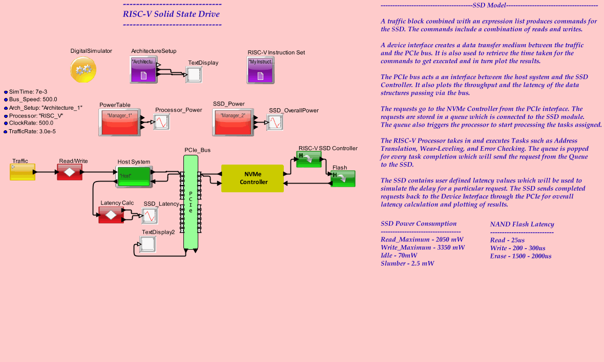
—————————————SSD Model Details—————————————
A traffic block combined with an expression list produces commands for the SSD. The commands include a combination of reads and writes.
A device interface creates a data transfer medium between the traffic and the PCIe bus. It is also used to retrieve the time taken for the commands
to get executed and in turn plot the results.
The PCIe bus acts a an interface between the host system and the SSD Controller. It also plots the throughput and the latency of the data structures passing via the bus.
The requests go to the NVMe Controller from the PCIe interface. The requests are stored in a queue which is connected to the SSD module. The queue also triggers the
processor to start processing the tasks assigned.
The RISC-V Processor takes in and executes Tasks such as Address Translation, Wear-Leveling, and Error Checking. The queue is popped for every task completion
which will send the request from the Queue to the SSD.
The SSD contains user defined latency values which will be used to simulate the delay for a particular request. The SSD sends completed requests back to the Device
Interface through the PCIe for overall latency calculation and plotting of results.
Use of the Cache block as the L2 cache, receiving request from the I_1 and D_1 in the processor and a miss to a DRAM.
Modeling the cycle-accurate cache with 4-way associativity and snoop flag disabled.
Shows an end-to-end operation with Processor core as a trace, 2 level cache, AXI bus, Memory Controller and DRAM
Use of the Cache block as the L2 cache, receiving request from the I_1 and D_1 in the processor and a miss to a DRAM.
Modeling multiple requester with addresses to DDR and LPDDR
Host computer with SATA interface to a local disk drive
Multi-level drive with cache, SDRAM, flash and disk drive. Uses a ARM R8 for contorl processing
Evaluate flash from different memory vendors by varying standard Flash parameters
Modeling a video streaming server that is stored on a redundant NAS


