The term dual channel refers to a double data rate (DDR) motherboards chip-set that’s designed with two memory channels instead of one. Dual-channel mode is a feature that was created to reduce the potential performance bottleneck that exists between the CPU and the DRAM. The memory modules are installed into matching slots, which are usually color-coded on the motherboard. These separate channels allow the memory controller access to each memory module. Dual-channel-enabled memory controllers is equally applicable for PC, SOC and Embedded system architecture and it utilize two 64-bit data channels, resulting in a total bandwidth of 128-bits, to move data from RAM to the CPU.
Dual Channel memory controllers are memory controllers where the DRAM devices are accessed from two different ports of the crossbar, PCIe or AXI bus. Both the memory controllers can access the DRAM in parallel. This doubles the theoretical bandwidth of the bus. It is targeted for high bandwidth access with high power capacity such as next-generation mobile, networking and consumer applications. The controller architecture is carefully tailored to achieve reliable high-frequency operation with dynamic power management and rapid system debug capabilities.
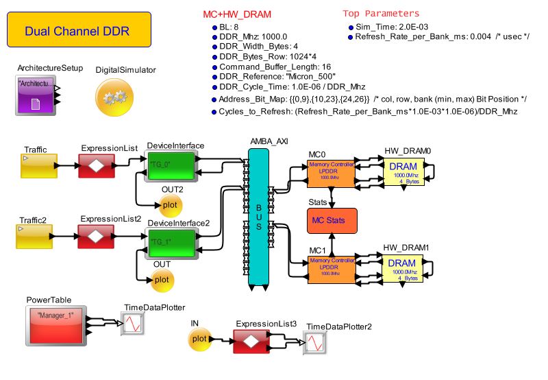
Fig 1. Dual Channel DDR in VisualSim
The dual channels handle memory-processing more efficiently by utilizing the theoretical bandwidth of the two modules, thus reducing system latencies, the timing delays that inherently occur with one memory interface. For example, an analogy in which data is filled into a funnel (memory), which then channels the data to the CPU. Single-channel memory would feed the data to the processor via a single funnel at a maximum rate of 64 bits at a time. Dual-channel memory, on the other hand, utilizes two funnels, thereby having the capability to deliver data twice as fast, at up to 128 bits at a time. The process works the same way when data is emptied from the processor by reversing the flow of data. A memory controller chip is responsible for handling all data transfers involving the memory modules and the processor. This controls the flow of data through the funnels, preventing them from being over-filled with data.
To evaluate the benefits of the dual channel memory for our system design, we assembled a system-level modeling using commercial software- VisualSim Architect from Mirabilis Design Inc. The flow of the model in VisualSim contains two Masters with equal access to both the DDR-DRAM. The first Master generates transaction and is connected to the Master Port of the AXI. This Master reads data from the first slave AXI bus port using the DDR3 controller. Similarly the second Master writes the data through bus interface to the second memory controller (DDR3). The width of the AXI bus is 4 bytes and the clock frequency is 500MHz. Both memory controllers are running at the same clock frequency and width. The first master targets the same row on all the Banks while the second Master performs random accesses. In the model, we generate an address that fits the address bit map and is used by the memory controller to breakdown into row, column and bank. This address is used to select the row-column in the DRAM. The memory controller has a request buffer that searches for the next sequential request. This way, the performance of the memory is optimized for minimal activate signals.
A list of the timing and performance characteristics of popular DDR3-DRAM component from Micron was assembled for the experiment. The model uses this file as input for the configuration of the timing of RCD, RP, RAS, CCD, WTR and RRD. In this model, the memory name refers to the micron 500 and this memory saves the power information for each state. It measures the statistics of the system power consumption for each memory. From this instant and average power outputs are analyzed (figure 4). The statistics output is display (figure 1) and their state plot are analyzed for two memories (figure 2 and 3). If the bandwidth of the DDR memory is increased, latency is reduced (as shown in the table-1 and refer figure 5 & 6).
Thus this model is done by using VisualSim Architect which is more efficient for users to provide large library and modelling different design with various attributes like time, power, latency and statistics report.
Below are given some example experiment results of the model on VisualSim software.
| Bandwidth of DDR (MHz) |
Latency (us) |
| 500 |
0.02 |
| 1000 |
0.016 |
| 2000 |
0.012 |
Table -1 (At peak point)
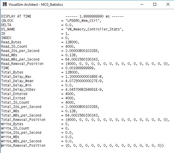
Fig 2. Statistics Output (Read)
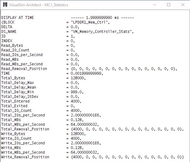
Fig 3. Output Statistics (Write)
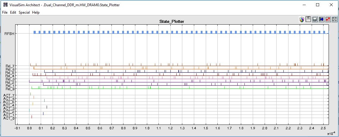
Fig 4. State Plot (DDR0)
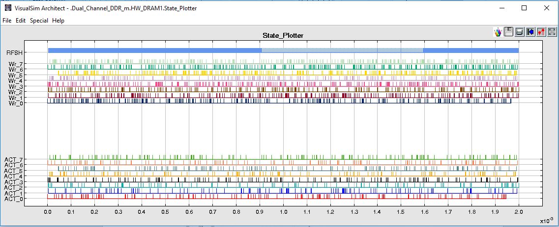
Fig 4. State Plot (DDR1)
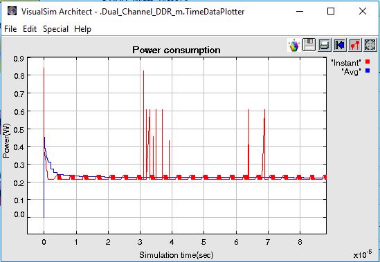
Fig 6. Power Performance
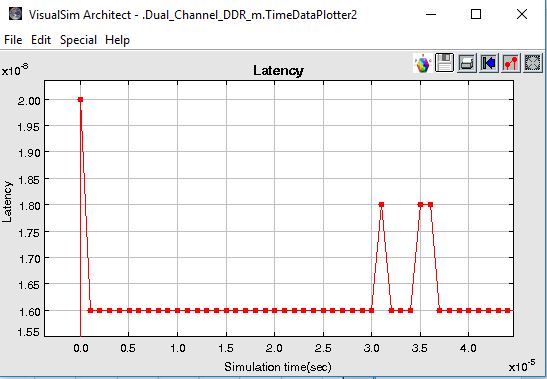
Fig 7. Latency at 500Mhz
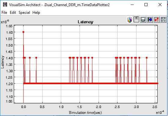
Fig 8. Latency at 1000 Mhz
Conclusion
Multiple DRAM channels certainly alleviate the bottleneck effect caused by the main memory bandwidth. System performance is largely dependent upon channel organization as well as program’s memory access pattern. Memory power consumption becomes more and more concerned in system design, especially for embedded systems, SOC, rapid system, next generation mobile and consumer applications. DDR2 SDRAM devices provides high data bandwidth with lower system power than DDR. When channel0 is serving an access, another access can be issued to channel1 and get served immediately, reducing access latency and provides better data throughput. Due to the doubled bandwidth, it takes half time to transfer requested memory blocks, yielding a high data throughput, although the latency of memory accesses is not directly affected. Thus, this model is done by VisualSim software which is used for performance trade-off analyses using such metrics as bandwidth utilization, application response time and buffer requirements. It is a graphical tool which provides large library and modelling different design with various attributes like time, power, latency and statistics report.