
The quality of signal processing systems such as a software defined radio or a communication modem is dependent on the performance of the selected hardware platform. Early design explorations enable the designer to gain insights into implementation challenges, architectural decisions to enhance performance and power, and hardware/software partitioning before Register-Transfer level (RTL) and software are available.
In addition, early design explorations assist architectural design decisions that facilitate planning for current and future requirements. Designers can further extend the design explorations to conduct fault analysis and identify test cases for verification.
This article presents the system level modelling and simulation methodology to architect a signal processing platform for software-defined radios or high-speed communication modems early in the design flow.
Problem
The majority of complex systems such as advanced high speed signal processing platforms go through expensive design iterations. Over 70% of the time iterations are due to incorrect design decisions or misunderstanding about the requirements. In addition, numerous factors influence such complex systems. A few of them are low processing latency, low power, configurability and limitations in resources. Early design explorations help overcome such issues.
Designers and architects follow number of ways to conduct design explorations and analysis. Though analytical methods provide significant information on the worst-case execution time, majority of the range do not occur in real life. Physical testing methods may provide accurate information, but are not feasible for complex systems such as SDRs or High Speed Communication modems.
Solution
Discrete event simulation enables designers and architects to evaluate a target system with hundreds or thousands of use cases, task scheduling, and system configurations in a shorter time frame. Discrete Event Modelling and Simulation helps not only in constructing extremely complex simulation models but also enables architects and designers to run extensive set of use cases and probabilities.
In addition, availability of pre-built and validated libraries of hardware architectural components and framework assist in modelling software architecture. They improve the accuracy of the system model and reduce the time to construct simulation models.
This approach allows designer to
- Focus on analysis and interpretation of results rather than constructing models.
- Optimize product architectures by running simulations with application profiles to explore platform selection; hardware versus software decisions; peripheral devices versus performance; and distribution of software threads on target architectures.
Solution Implementation
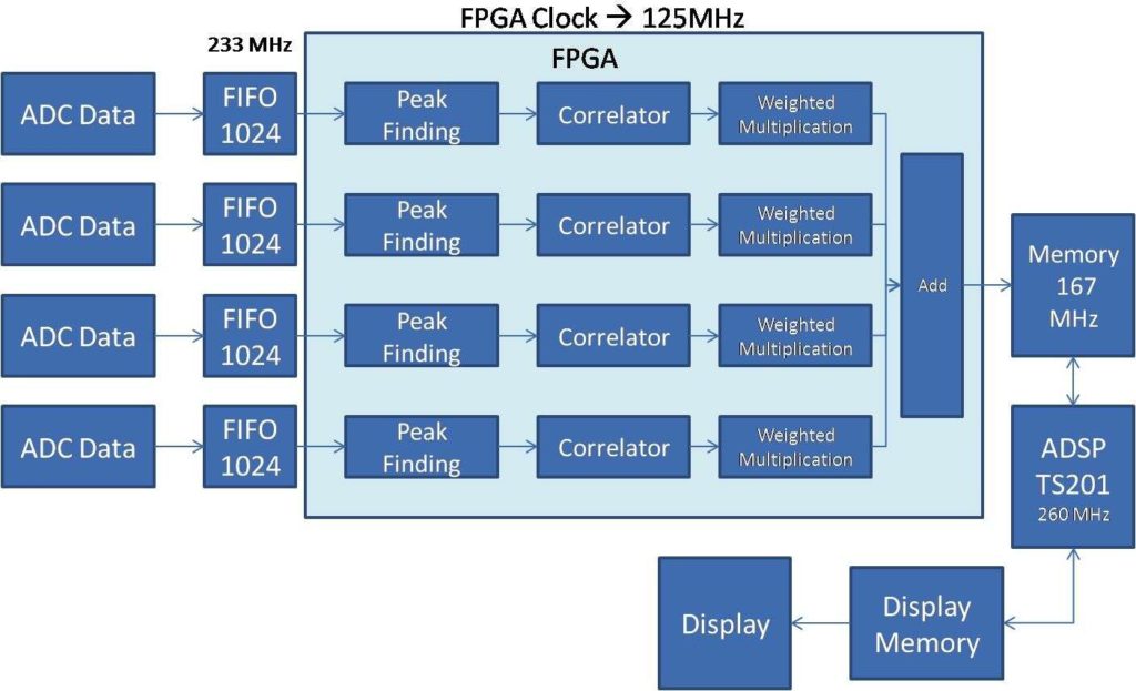
This article presents the design exploration of a signal processing platform. The purpose of the design explorations is to capture processing latency, Field-Programmable Gate Array (FPGA) Buffer Requirements, impact of packet length on performance, and identification of hardware platform configurations. The explorations can be further extended to understand resource utilizations for each signal processing functions such as peak finding, correlator, weighted multiplications, and accumulator.
The discrete event simulation model utilizes the following components:
- Four ADC Channels at 5 MHz.
- Packet Length of 512 and 1024 Bytes.
- FIFO at 233 MHz.
- Buffer with a Depth of 1024.
- FPGA Initial Clock Speed is 125MHz. FPGA Clock Speed can be varied to meet latency requirements.
- External DDR Memory running at 167 MHz.
- ADSP TS201 running at 260MHz.
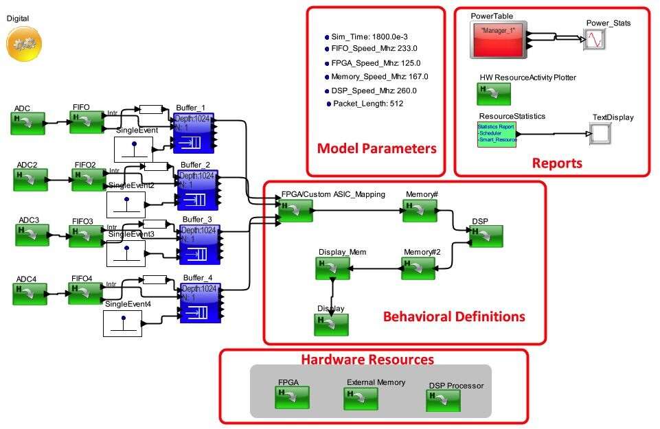
Models are constructed graphically using VisualSim Architect’s pre-built configurable libraries. Processors, memory, FPGA Resources, Buses and Interconnects are modelled using VisualSim “SystemResource” library blocks. Analog-to-digital Converters (ADCs) are modelled as traffic generators and are responsible for generating digital samples at 5MHz.
In this system exploration, we considered abstract details for each function. The details can be leveraged to create an elaborate model by integrating matlab/simulink/C/C++ modules. For each function, we have considered timing values from existing Verilog code running in system generator and standard published values. Sum of weighted inputs are forwarded to Digital Signal Processor for display processing and floating point FFT and then the data is written into Frame Buffer for display.
Block diagram of the proposed system platform is shown in figure 1 and the VisualSim simulation model is shown in figure 2.
Analysis and Reports
The model was constructed in two person hours and the simulation was run on a 2.6 GHz Microsoft Windows 10 platform with 4 GB RAM, simulating 900.0 msec of real time. VisualSim took 25 seconds of wall clock time to finish a simulation.
Explorations are focused on achieving algorithm processing deadline time based on the packet size and capture power versus performance trade-off.
Analysis 1
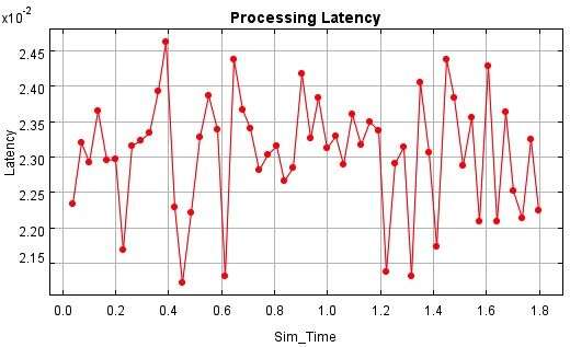
This exploration considers buffer depth as twice the size of “Packet Length” and expects signal processing latency for a packet length of 512 bytes to be under 20 ms.
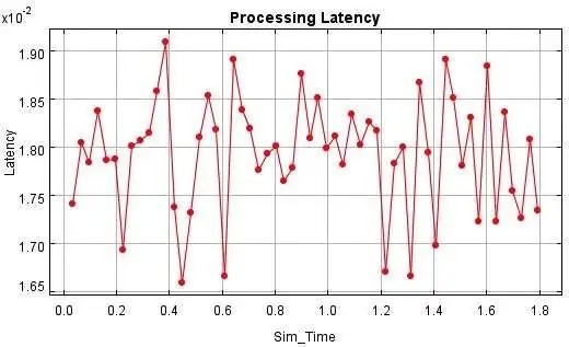
The simulation reports displayed in figure 3 show that the maximum processing latency is of 24.52 ms. This states that the Signal Processing functions implemented on FPGA take more cycles to process. The solution to overcome this challenge is to either increase the clock speed of FPGA or modify the algorithm. We decided to increase the clock speed of the FPGA as a preliminary solution.
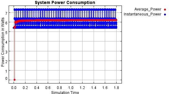
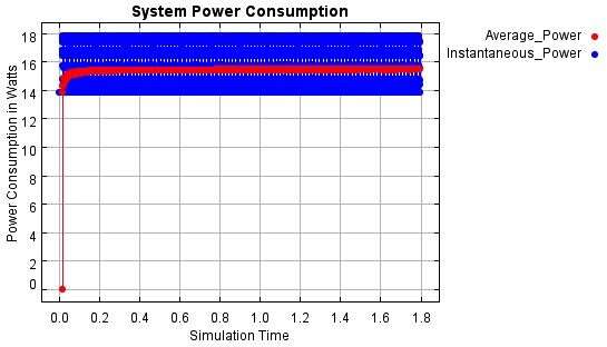
With successive explorations, we identified that by increasing FPGA clock speed from 125 MHz to 170MHz, system meets latency requirements of 20 ms. We have identified that the average power consumption (6.2 Watts) increased merely by 1.1 Watts.
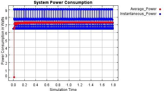
The latency graph is shown in figure 5 and power consumption graph is shown in figure 6.
Considering possibilities of requirements in increased Packet Length support, we extended system analysis by increasing the packet length from 512 bytes to 2048 bytes. We identified no significant changes in power consumption. However, the achieved maximum processing latency was 76 ms as opposed to expected latency of 20ms or less. Average Power consumption of the system reported was 7.8 Watts.
We also looked at the buffer occupancy for certain functions. Buffer occupancy in number of packets count for each function show in Table 1 for all the above scenarios is identical. This suggests that the algorithm implementation is not optimized to support variations in Packet Size and also implementation is not feasible if the design requires variable packet size.
| Function | Buffer in Number of Packets Count |
| Peak Finding/Pre-Processing | 4 * Packet Size |
| Correlator | 4 * Packet Size |
| Weighted Multiplication | 3 * Packet Size |
| Sum | 1 * Packet Size |
Table 1: Buffer Requirements
Analysis 2
During this exploration, we modeled dedicated resources for each function per ADC channel.
We looked at the processing latency graph and average power consumption graph to evaluate system configurations.
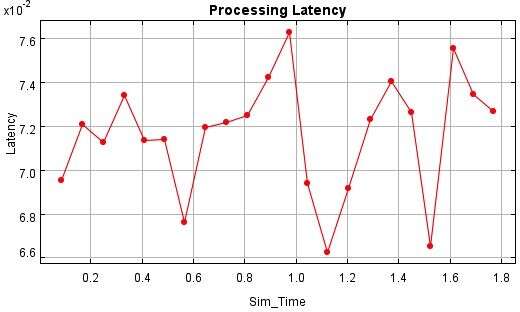
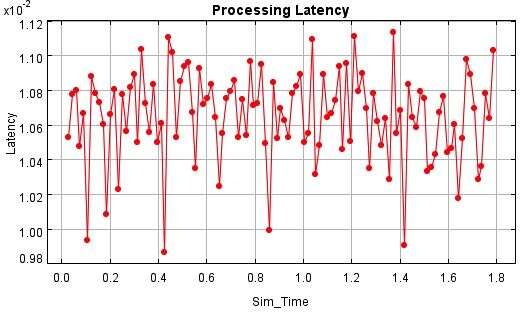
The processing latency is shown in figure 8 and average system power consumption is shown in figure 9.
As each function per ADC channel has dedicated FPGA resources, the power consumption of the system increases considerably as compared to average system power consumption shown in Analysis 1. However average end-to-end latency is below 10.8 milliseconds with a peak latency of 11.1 milliseconds.
This shows that the performance requirements can be met even at lesser FPGA clock speed if dedicated FPGA resources are being considered for each ADC Channel.
On the down side, we noticed that the FPGA resource requirements are more and also average power consumption increased by 100%.
Conclusion
Early design explorations with modelling and simulation validate the hardware capability and efficiency to implement signal processing algorithms. This ensures that the selected architecture has sufficient processing power to meet current and future requirements in terms of performance, power, and reliability of the system. Performance modelling with VisualSim enabled us to estimate resource requirements, performance, and power statistics to make design decisions.
In our studies, we identified that with “Analysis – 1”, system architect can make design decisions balancing both performance and power consumption of the system. “Analysis – 2” shows that the system performance can be achieved even with lower clock speeds but requires more FPGA resources and almost 100% more power requirements.
The explorations can be extended further by constructing cycle accurate models of the hardware resources and investigation at micro-architecture level.
References
- R.S. Janka, L.M. Wills, et al.,”Virtual benchmarking and model continuity in prototyping embedded multiprocessor signal processing systems”, IEEE, 2002
- S. Kapralov, V. Dyankova, “Modeling a System with Discrete Events”, IEEE, 2012
- Sundeep Lal, Roberto Muscedere, et al., “An FPGA-based signal processing system for a 77 GHz MEMS tri-mode automotive radar”, IEEE, 2011
- K. Puttaswamy, Kyu-Won Choi, et al., “System level power-performance trade-offs in embedded systems using voltage and frequency scaling of off-chip buses and memory”, IEEE, 2005
- Stephen Bijansky, Bassam Mohd, Baker Mohammad, “Dynamic power analysis for custom design”, IEEE, 2009
- VisualSim Architect Product Documentation, Mirabilis Design Inc., 2016
Keywords: system-level IP, power measurement, EDA tools, semiconductors, signal processing systems, Register-Transfer level, RTL, early design explorations, High Speed Communication modems, SDR, Discrete event simulation, Field-Programmable Gate Array, FPGA, Analog-to-digital Converters, ADC, Packet Length, clock speed, power consumption, Peak Finding, Correlator, Weighted Multiplication, Sum, Design Methods


