
Abstract
The jump from 3G to 4G was significant because of the control logic requirements that made the standard way to exploring the algorithm difficult. From the hardware-software architecture, the introduction of hardware accelerators and the integration of DSP, uP and GPU enabled companies to transition to the new speeds, modulation, antenna, and microware design.
5G and 6G personalizes control logic, creates dynamic task instances based on intelligent processing, and requires a large pool of processing resources. The decisions are made based on significant amount of AI/ML learning.
The selection of the modulation schemes for a particular users depends on the call setup by the upper layers of the protocol stack and the protocol layer makes its decision based on the traffic stream, channel quality and the available AI/DSP resources. Similarly, the antenna loss can be very high if not aligned with the Transceiver.
All of these point to a completely new form of architecture and system design methodology.
Overview of 5G/6G system behavior
For the 5G/6G, the software behavior is very different. The task flow dynamically generates multiple instances of tasks based on the user-type, bandwidth requirements and types of processing. The wireless modem hardware is made up of many small AI or DSP cores. The system must optimally use this resource to keep power down, but still maintain the performance. For extremely low-cost, a processor can be used but the software would have to be multi-threaded and can be fairly complex.
To get a true picture, we would have to model the protocol stack and physical baseband to determine the control (protocol) and the execution requirements (baseband). The AI, DSP and other hardware resources would need to be modeled as a pool of resources. Depending on the number of active instances of each task, there will be a variable number of AI/DSP requests. The system should quickly move multiple resources from Deepsleep to Active to ensure that the timing deadline is maintained.
Architects are not familiar with the mathematics of the baseband algorithms. On the other hand, they do need to provide information to the software developer on the constraints that they need to implement within.
The true power consumption can only be estimated if we incorporate the peripherals, interfaces, microwave and the antenna. This means that the system designer must also deal with these technologies. The challenge is to find a platform where all these can be evaluated at the same time. But the systems engineer will not be familiar with the implementation details, solvers and optimization needs.
VisualSim Mixed-Signal Semiconductor and Systems Evaluator from Mirabilis Design is a unique simulation and IP library of architecture, signal and functional library components to rapidly assemble model of the system from sensor to antenna, within the semiconductor device or a large distributed system. VisualSim Evaluator can be used by mixed-signal teams, RF Architects, communication designers, and system engineers to evaluate individual component in the context of a complete mixed-signal or communication system behavior (sensors, interfaces, protocol, physical baseband, analog, RF, antenna, and channel). System designers can test the feasibility of a proposal or verify the correctness of the implementation by varying the frequencies, distances, signal strength, path loss, RF gain, multi-antenna scenario, modulation schemes, encryption, and channel types. The goal is to gain a complete understanding of the system behavior and create a traceable platform to verify the implementation.
Note: VisualSim Evaluator was granted the Best in Show Award at Embedded World 2022.
Today’s design platform for mixed signal simulation is highly disjointed. For the system designer, they need extensive knowledge of the underlying microwave and signal processing theory to define the system. There is no signal view of the semiconductor and associated system. There are separate tools, flows and methodology for the Antenna, RF/Microwave, mixed-signal, signal processing, protocols and digital sub-systems. Current point-tools solution work on specific functional blocks and provide signal-level or physical-level behaviors only. There is no single tool to assemble the architecture for the entire semiconductor device. Moreover, this sensor or mixed signal design flow cannot be integrated into the full system that contains batteries, power systems, processors, and interfaces. Lastly the expected rates and values at the different interfaces cannot be completely tested.
| Key features | |
| –Technology library contains RF Generators, Antenna, Baseband, Microwave, DAC/ADC, Filters, Channel, Tx/Rx, interface and sensors -Simulate Mixed-Signal and communication Based on Datasheet without manufacturers proprietary details or underlying theory -Conduct Feasibility Test in system environment on performance, prior to design –Configure a multiple silicon model without designing individual components in the system –Simulate Real World system performance in user’s desired system as Test-before-Build | –Fully integrated with the VisualSim Cloud to easily create an online catalog of devices for rapid system prototyping and selection -Connect architects, Mixed-Signal teams, systems engineers, signal engineers, verification engineers, and Customers -Evaluate based on application rather than the signal behavior, physical characteristics and Type –Used in planning and post design validation phase of the product development cycle -Eliminates Exclusivity of mixed-signal Simulation for microwave experts only |
The lack of a single flow and platform causes miscommunication, and the area, power consumed, response time and throughput cannot be easily measured. Debugging such a system relies on emulation or with the physical device. Both scenarios happen very late in the design process and make it very difficult to incorporate changes. Also, full-chip verification is difficult because the different parts of the semiconductor are not integrated until the very end of the project. VisualSim Mixed-Signal Designers provides a single platform that can capture the architecture from sensor to antenna to include the microwave, signal processing and interfaces, sensors and digital processing. These models are defined using a combination of delays, power consumption, loss/gain db, equations that emulate the sequence of operation, frequency of operation, expected data rates and processing requirements. Using these models, the user can test the feasibility, maximum data rate, expected latency and power consumed. Once the requirements of each block have been established, the functional blocks can be refined with the signal processing, filtering, and other manipulation of the data. The signal-level mathematics can be performed either using an established software such as Simulink and ADS or developed using the VisualSim library blocks. Each individual block can be tested in the context of the entire semiconductor SoC.
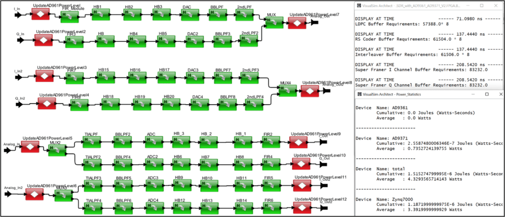
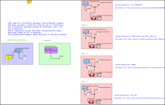
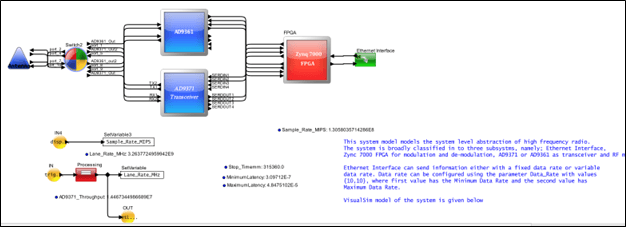
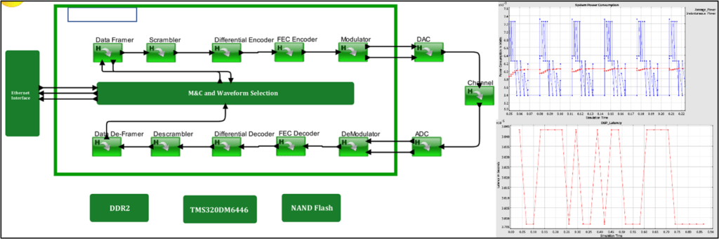
VisualSim Mixed-Signal Evaluator has several applications including A-to-D and D-to-A intelligent semiconductor, advanced radar systems and mixed-signal semiconductor, autonomous driving systems from sensor to processing, 5G mobile and base stations, and other communication systems.
To understand the application of the VisualSim Mixed Signal Evaluation, consider a Radar system that is used in aircrafts for enemy plane tracking and in autonomous driving vehicles for pedestrian tracking. A radar system has an antenna, RF Tx/Rx, DAC/ADC, filtering, signal processing, control processing, decision intelligence, recording and storage. The system is integrated into the rest of the system through a Gigabit Ethernet or HDMI interface. From a design standpoint, the user will
- Define the end-to-end architecture that includes the channel, antenna, DAC/ADC, RF Tx/Rx, filter, modulator, encryption, storage, processing, interconnect, sensors, and interfaces
- Add the implementation, timing, power consumption and behavior details for components
- Measure performance metrics (gain, carrier and rf frequency, response times, power consumed, filtering, data rate) for each component and end-to-end system
- Use measurement to define the requirements for each functional blocks within the components. This includes mixed-signal, digital processing and thermal systems.
- Develop the signal and physical models in VisualSim or other software such as ADS and Simulink
- Enhance the architecture model with these signal models to test the end-to-end functional correctness
- Replace the functional blocks with circuit models or emulation for verification. Alternately generate test benches for verification in the native implementation environment
- Provide the mixed-signal architecture model to the automotive or avionics manufacturer for designing the full-system
VisualSim Mixed-Signal Designers enables uniform communication across the entire team. Before any mathematical or implementation development, the team can estimate the required amplification, data rates, processing speed, processing times, power consumed, required area, processing constraints and other requirements. The continuous validation of the functional blocks from concept to deployment ensures traceability and ensures capturing of errors and faults. Also, the architecture model can be shared with customers to assemble the full system, prior to the silicon becoming available.
Keywords: Mixed-Signal, Antenna, RF/Microwave, Analog, Signal Processing, Baseband, Digital Hardware, Protocols stack, software, systems engineering, architecture exploration, mathematical modeling, modeling and simulation


