Display Systems

Selecting the components for a multi-display system with sensor, video encoding and front-end display processing

TMS320DM6437_1

Browsable image of the model.

  • For an executable version,
  • Mouse over the icons to view parameters. Click on hierarchy and plotters to reveal content (if provided).
  • To simulate, click on Launch button, open downloaded file and click Run on the Java Security Page.
TMS320DM6437_1model <h2>Latency2</h2><table border="1"><tr><td><b>Parameter</b></td><td><b>Expression</b></td><td><b>Value</b></td></tr><tr><td>Block_Documentation</td><td>Enter User Documentation Here</td><td>Enter User Documentation Here</td></tr><tr><td>Frame_Time</td><td>1.0 / FPS /* DO NOT MODIFY */</td><td>0.005</td></tr></table> <h2>Latency_Out2</h2><table border="1"><tr><td><b>Parameter</b></td><td><b>Expression</b></td><td><b>Value</b></td></tr><tr><td>Block_Documentation</td><td>Enter User Documentation Here</td><td>Enter User Documentation Here</td></tr><tr><td>_flipPortsHorizontal</td><td>true</td><td>true</td></tr></table> <h2>VideoEncode2</h2><table border="1"><tr><td><b>Parameter</b></td><td><b>Expression</b></td><td><b>Value</b></td></tr><tr><td>Block_Documentation</td><td>Enter User Documentation Here</td><td>Enter User Documentation Here</td></tr><tr><td>Device_Name</td><td>&quot;VE&quot;</td><td>&quot;VE&quot;</td></tr><tr><td>Cycle_Time</td><td>1.0E-06/VPSS_Speed_Mhz</td><td>2.4691358024691E-9</td></tr><tr><td>Width_Bytes</td><td>4</td><td>4</td></tr><tr><td>DRAM_Name</td><td>&quot;DRAM&quot;</td><td>&quot;DRAM&quot;</td></tr></table> <h2>OSD2</h2><table border="1"><tr><td><b>Parameter</b></td><td><b>Expression</b></td><td><b>Value</b></td></tr><tr><td>Block_Documentation</td><td>Enter User Documentation Here</td><td>Enter User Documentation Here</td></tr><tr><td>FPS</td><td>33.0e6/(Image_Bytes/8)</td><td>1527.7777777777778</td></tr><tr><td>Frame_Time</td><td>1.0 / FPS /* DO NOT MODIFY */</td><td>6.5454545454545E-4</td></tr><tr><td>Image_Bytes</td><td>Image_Bytes*2</td><td>172800</td></tr><tr><td>_flipPortsHorizontal</td><td>true</td><td>true</td></tr><tr><td>Cycle_Time</td><td>1.0E-06/VPSS_Speed_Mhz</td><td>2.4691358024691E-9</td></tr><tr><td>Width_Bytes</td><td>4</td><td>4</td></tr></table> <h2>Switch2</h2><table border="1"><tr><td><b>Parameter</b></td><td><b>Expression</b></td><td><b>Value</b></td></tr><tr><td>Block_Documentation</td><td>Enter User Documentation Here</td><td>Enter User Documentation Here</td></tr></table> <h2>Resizer2</h2><table border="1"><tr><td><b>Parameter</b></td><td><b>Expression</b></td><td><b>Value</b></td></tr><tr><td>Block_Documentation</td><td>Enter User Documentation Here</td><td>Enter User Documentation Here</td></tr><tr><td>Device_Name</td><td>&quot;Resizer&quot;</td><td>&quot;Resizer&quot;</td></tr><tr><td>Cycle_Time</td><td>1.0E-06/VPSS_Speed_Mhz</td><td>2.4691358024691E-9</td></tr><tr><td>Width_Bytes</td><td>4</td><td>4</td></tr><tr><td>DRAM_Name</td><td>&quot;DDR3DRAM_2&quot;</td><td>&quot;DDR3DRAM_2&quot;</td></tr></table> <h2>Previewer2</h2><table border="1"><tr><td><b>Parameter</b></td><td><b>Expression</b></td><td><b>Value</b></td></tr><tr><td>Block_Documentation</td><td>Enter User Documentation Here</td><td>Enter User Documentation Here</td></tr><tr><td>Device_Name</td><td>&quot;Previewer&quot;</td><td>&quot;Previewer&quot;</td></tr><tr><td>Cycle_Time</td><td>1.0E-06/VPSS_Speed_Mhz</td><td>2.4691358024691E-9</td></tr><tr><td>DRAM_Name</td><td>&quot;DDR3DRAM_2&quot;</td><td>&quot;DDR3DRAM_2&quot;</td></tr><tr><td>Width_Bytes</td><td>4</td><td>4</td></tr></table> <h2>Image_Sensor2</h2><table border="1"><tr><td><b>Parameter</b></td><td><b>Expression</b></td><td><b>Value</b></td></tr><tr><td>Block_Documentation</td><td>Enter User Documentation Here</td><td>Enter User Documentation Here</td></tr><tr><td>FPS</td><td>54.0e6/(Image_Bytes/8)</td><td>5000.0</td></tr><tr><td>Frame_Time</td><td>1.0 / FPS /* DO NOT MODIFY */</td><td>2.0E-4</td></tr><tr><td>Image_Bytes</td><td>Image_Bytes</td><td>86400</td></tr></table> <h2>CCDC2</h2><table border="1"><tr><td><b>Parameter</b></td><td><b>Expression</b></td><td><b>Value</b></td></tr><tr><td>Block_Documentation</td><td>Enter User Documentation Here</td><td>Enter User Documentation Here</td></tr><tr><td>Device_Name</td><td>&quot;CCDC&quot;</td><td>&quot;CCDC&quot;</td></tr><tr><td>Cycle_Time</td><td>1.0E-06/VPSS_Speed_Mhz</td><td>2.4691358024691E-9</td></tr><tr><td>Width_Bytes</td><td>8</td><td>8</td></tr><tr><td>DRAM_Name</td><td>&quot;DDR3DRAM_1&quot;</td><td>&quot;DDR3DRAM_1&quot;</td></tr></table> <h2>H3A2</h2><table border="1"><tr><td><b>Parameter</b></td><td><b>Expression</b></td><td><b>Value</b></td></tr><tr><td>Block_Documentation</td><td>Enter User Documentation Here</td><td>Enter User Documentation Here</td></tr><tr><td>Device_Name</td><td>&quot;H3A&quot;</td><td>&quot;H3A&quot;</td></tr><tr><td>Cycle_Time</td><td>1.0E-06/VPSS_Speed_Mhz</td><td>2.4691358024691E-9</td></tr><tr><td>Width_Bytes</td><td>8</td><td>8</td></tr><tr><td>DRAM_Name</td><td>&quot;DDR3DRAM_1&quot;</td><td>&quot;DDR3DRAM_1&quot;</td></tr></table> <h2>Histogram2</h2><table border="1"><tr><td><b>Parameter</b></td><td><b>Expression</b></td><td><b>Value</b></td></tr><tr><td>Block_Documentation</td><td>Enter User Documentation Here</td><td>Enter User Documentation Here</td></tr><tr><td>FPS</td><td>FPS</td><td>200</td></tr><tr><td>Frame_Time</td><td>1.0 / FPS /* DO NOT MODIFY */</td><td>0.005</td></tr><tr><td>Image_Bytes</td><td>Image_Bytes</td><td>86400</td></tr><tr><td>_flipPortsHorizontal</td><td>true</td><td>true</td></tr><tr><td>Cycle_Time</td><td>1.0E-06/VPSS_Speed_Mhz</td><td>2.4691358024691E-9</td></tr><tr><td>Width_Bytes</td><td>8</td><td>8</td></tr></table> <h2>TextDisplay</h2><table border="1"><tr><td><b>Parameter</b></td><td><b>Expression</b></td><td><b>Value</b></td></tr><tr><td>Block_Documentation</td><td>Enter User Documentation Here</td><td>Enter User Documentation Here</td></tr><tr><td>rowsDisplayed</td><td>10</td><td>10</td></tr><tr><td>columnsDisplayed</td><td>40</td><td>40</td></tr><tr><td>suppressBlankLines</td><td>false</td><td>false</td></tr><tr><td>title</td><td>&quot;Detailed Processor Activity&quot;</td><td>&quot;Detailed Processor Activity&quot;</td></tr><tr><td>ViewText</td><td>true</td><td>true</td></tr><tr><td>saveText</td><td>false</td><td>false</td></tr><tr><td>fileName</td><td>Enter Filename to save text</td><td>&quot;Enter Filename to save text&quot;</td></tr><tr><td>Append_Time</td><td>true</td><td>true</td></tr></table> <h2>RTOS</h2><table border="1"><tr><td><b>Parameter</b></td><td><b>Expression</b></td><td><b>Value</b></td></tr><tr><td>Block_Documentation</td><td>Enter User Documentation Here</td><td>Enter User Documentation Here</td></tr></table> <h2>HW_DRAM</h2><table border="1"><tr><td><b>Parameter</b></td><td><b>Expression</b></td><td><b>Value</b></td></tr><tr><td>Architecture_Name</td><td>&quot;Architecture_1&quot;</td><td>&quot;Architecture_1&quot;</td></tr><tr><td>HW_DRAM_Name</td><td>&quot;DRAM&quot;</td><td>&quot;DRAM&quot;</td></tr><tr><td>HW_DRAM_Speed_Mhz</td><td>166.0</td><td>166.0</td></tr><tr><td>Number_of_Banks</td><td>8</td><td>8</td></tr><tr><td>Sim_Time</td><td>Sim_Time</td><td>0.15</td></tr><tr><td>_explanation</td><td>Hardware_Modeling-&gt;Memory-&gt;HW_DRAM</td><td>Hardware_Modeling-&gt;Memory-&gt;HW_DRAM</td></tr><tr><td>Memory_Width_Bytes</td><td>4</td><td>4</td></tr><tr><td>Burst_Length</td><td>4 /* 2, 4, 8 */</td><td>4</td></tr><tr><td>DRAM_Type</td><td>&quot;DDR&quot; /* SDR, DDR, DDR2, LPDDR, LPDDR2_NV, LPDDR2_S2, LPDDR2_S4, DDR3 */</td><td>&quot;DDR&quot;</td></tr><tr><td>Mfg_Suggest_Timing</td><td>{2,2,2,6} /* tCAS, tRCD, tRP, tRAS */</td><td>{2, 2, 2, 6}</td></tr><tr><td>Extra_Timing</td><td>{2,2,1,1,3,1,2,1,0,16} /* DQSS, tWTR, tRRD, tWR, tRL, tWL , tDQSCK, tRTP, tHWpre, tFAW */</td><td>{2, 2, 1, 1, 3, 1, 2, 1, 0, 16}</td></tr><tr><td>Fix_DQSS</td><td>true</td><td>true</td></tr><tr><td>Refresh_Rate_per_Bank_ms</td><td>64.0 /* 64.0 ms */</td><td>64.0</td></tr><tr><td>Refresh_Cycles_per_Bank</td><td>256 /* 256 cycles per bank */</td><td>256</td></tr><tr><td>Enable_External_Data</td><td>false</td><td>false</td></tr><tr><td>Address_Bit_Map</td><td>{{0,9},{10,24},{25,27}}  /* col, row, bank (min, max) Bit Position */</td><td>{{0, 9}, {10, 24}, {25, 27}}</td></tr><tr><td>Standard_Name</td><td>&quot;none&quot; /*reads DDR_Memory_Standards.txt */</td><td>&quot;none&quot;</td></tr><tr><td>Standard_File</td><td>VS/VisualSim/actor/arch/Memory/DDR_Memory_Standards.txt</td><td>&quot;VS/VisualSim/actor/arch/Memory/DDR_Memory_Standards.txt&quot;</td></tr><tr><td>Power_Manager_Name</td><td>&quot;none&quot;  /* Default */</td><td>&quot;none&quot;</td></tr><tr><td>Memory_Controller</td><td>&quot;none&quot;  /* Default */</td><td>&quot;none&quot;</td></tr><tr><td>Bank_at_a_Time</td><td>true  /* false=all */</td><td>true</td></tr><tr><td>DEBUG</td><td>false</td><td>false</td></tr><tr><td>State_Plot_Enable</td><td>false</td><td>false</td></tr></table> <h2>Memory_Controller</h2><table border="1"><tr><td><b>Parameter</b></td><td><b>Expression</b></td><td><b>Value</b></td></tr><tr><td>Architecture_Name</td><td>&quot;Architecture_1&quot;</td><td>&quot;Architecture_1&quot;</td></tr><tr><td>Controller_Name</td><td>&quot;DDR&quot;</td><td>&quot;DDR&quot;</td></tr><tr><td>DRAM_Type</td><td>&quot;DDR&quot; /* SDR, DDR, DDR2, LPDDR, LPDDR2_NV, LPDDR2_S2, LPDDR2_S4, DDR3 */</td><td>&quot;DDR&quot;</td></tr><tr><td>Controller_Speed_Mhz</td><td>RAM_Speed_Mhz</td><td>166.0</td></tr><tr><td>Memory_Width_Bytes</td><td>4</td><td>4</td></tr><tr><td>Bus_Width_Bytes</td><td>8</td><td>8</td></tr><tr><td>Command_Buffer_Length</td><td>16</td><td>16</td></tr><tr><td>Commands_in_a_Row</td><td>8</td><td>8</td></tr><tr><td>Mfg_Suggest_Timing</td><td>{3,7,8,17} /* tCL, tRCD, tRP, tRAS */</td><td>{3, 7, 8, 17}</td></tr><tr><td>Extra_Timing</td><td>{1,3,4,1,3,1,1,1,0} /* DQSS, tWTR, tRRD,tWR, tRL, tWL, tDQSCK, tRTP, tHWpre */</td><td>{1, 3, 4, 1, 3, 1, 1, 1, 0}</td></tr><tr><td>Burst_Length</td><td>4 /* 2, 4, 8 */</td><td>4</td></tr><tr><td>Memory_Column</td><td>{0,21} </td><td>{0, 21}</td></tr><tr><td>Memory_Row</td><td>{22,29} </td><td>{22, 29}</td></tr><tr><td>Memory_Bank</td><td>{30,31}</td><td>{30, 31}</td></tr><tr><td>Memory_Bank_Length</td><td>round(pow(2,(Memory_Bank(1) - Memory_Bank(0) + 1)))</td><td>4L</td></tr><tr><td>DRAM_Return_Cycles</td><td>0</td><td>0</td></tr><tr><td>First_Word_Flag</td><td>true</td><td>true</td></tr><tr><td>Sim_Time</td><td>Sim_Time</td><td>0.15</td></tr><tr><td>Custom_Arbiter_File</td><td>&quot;none&quot;</td><td>&quot;none&quot;</td></tr><tr><td>Custom_Arbiter_Path</td><td>&quot;none&quot;</td><td>&quot;none&quot;</td></tr><tr><td>DEBUG</td><td>false</td><td>false</td></tr><tr><td>_explanation</td><td>Hardware_Modeling-&gt;Memory-&gt;Memory_Controller</td><td>Hardware_Modeling-&gt;Memory-&gt;Memory_Controller</td></tr><tr><td>HW_DRAM_Name</td><td>&quot;DDR0&quot;</td><td>&quot;DDR0&quot;</td></tr><tr><td>Power_Manager_Name</td><td>&quot;none&quot;  /* Default */</td><td>&quot;none&quot;</td></tr></table> <h2>Instruction_Set</h2><table border="1"><tr><td><b>Parameter</b></td><td><b>Expression</b></td><td><b>Value</b></td></tr><tr><td>Block_Documentation</td><td>Enter User Documentation Here</td><td>Enter User Documentation Here</td></tr><tr><td>Instruction_Set_Name</td><td>&quot;C64_Instr&quot;</td><td>&quot;C64_Instr&quot;</td></tr><tr><td>_explanation</td><td>ProcessorGenerator-&gt;Instruction_Set</td><td>ProcessorGenerator-&gt;Instruction_Set</td></tr><tr><td>Instruction_Set_Text</td><td>/* Instruction Set or File Path. */\\n   Mnew Ra  Rb  Rc  Rd   Re ;   /* Label */\\n   DSP  LUnit MUnit SUnit DUnit         ;\\n   LUnit  INT_1 INT_2         \t\t;\\n   MUnit  INT_3 INT_4               \t;\\n   SUnit  INT_5 INT_6                \t;\\n   DUnit  INT_7 INT_8\t\t\t;\\n\\nbegin INT_7                 ;   /* Group */\\nADD 1 ;\\nAND 1 ;\\nMV   1 ;\\nOR   1 ;\\nSTB  1 ;\\nLDB   5 ;\\nSUB  1 ;\\nXOR  1 ;\\nZERO 1 ;\\nend   INT_7                 ;\\n\\nbegin INT_8                 ;   /* Group */\\nADD 1 ;\\nAND 1 ;\\nMV   1 ;\\nOR   1 ;\\nSTB  1 ;\\nLDB   5 ;\\nSUB  1 ;\\nXOR  1 ;\\nZERO 1 ;\\nend   INT_8                 ;\\n\\nbegin INT_3                 ;   /* Group */\\nAVG 2 ;\\nMPY 1 ;\\nSSHVL  2 ;\\nBIT 2 ;\\nXORMPY 4 ;\\nXPND 2 ;\\nCMPY 3 ;\\nDDOTP 4 ;\\nDEAL 2 ;\\nMVD  4 ;\\nROTL 2 ;\\nSHFL 2 ;\\nend   INT_3                 ;\\n\\nbegin INT_4                 ;   /* Group */\\nAVG 2 ;\\nMPY 1 ;\\nSSHVL  2 ;\\nBIT 2 ;\\nXORMPY 4 ;\\nXPND 2 ;\\nCMPY 3 ;\\nDDOTP 4 ;\\nDEAL 2 ;\\nMVD  4 ;\\nROTL 2 ;\\nSHFL 2 ;\\nend   INT_4                 ;\\n\\nbegin INT_5                 ;   /* Group */\\nADD 1 ;\\nAND 1 ;\\n*B  5 ;\\nDMV  1 ;\\nSET 1 ;\\nMIN 1 ;\\nSHL  1 ;\\nMV  1 ;\\nSHR  1 ; \\nNEG 1 ;\\nOR  1 ;\\nPACK 1 ;\\nSUB 1 ;\\nCLR 1 ;\\nCMP 1 ;\\nSWAP 1 ;\\nUNPKHU4  1 ;\\nXOR 1 ;\\nZERO  1 ;\\nend   INT_5                  ;\\n\\nbegin INT_6                 ;   /* Group */\\nADD 1 ;\\nAND 1 ;\\n*B  5 ;\\nDMV  1 ;\\nSET 1 ;\\nMIN 1 ;\\nSHL  1 ;\\nMV  1 ;\\nSHR  1 ; \\nNEG 1 ;\\nOR  1 ;\\nPACK 1 ;\\nSUB 1 ;\\nCLR 1 ;\\nCMP 1 ;\\nSWAP 1 ;\\nUNPKHU4  1 ;\\nXOR 1 ;\\nZERO  1 ;\\nend   INT_6                  ;\\n\\nbegin INT_1                  ;   /* Group */\\nADD 1 ;\\nABS 1  ;\\nAND 1 ;\\nMIN 1 ; \\nSHL 1 ;\\nMV  1 ;\\nSUB 1 ;\\nNEG 1 ;\\nNORM 1 ;\\nNOT  1 ; \\nOR  1 ;\\nPACK 1 ;\\nCMP 1 ;\\nSWAP 1 ;\\nUNPKHU 1 ;\\nXOR 1 ;\\nZERO  1 ;\\nLMBD  1 ;\\nSAT 1 ;\\nMAX 1 ;\\nend   INT_1                  ;\\n\\nbegin INT_2                  ;   /* Group */\\nADD 1 ;\\nABS 1  ;\\nAND 1 ;\\nMIN 1 ; \\nSHL 1 ;\\nMV  1 ;\\nSUB 1 ;\\nNEG 1 ;\\nNORM 1 ;\\nNOT  1 ; \\nOR  1 ;\\nPACK 1 ;\\nCMP 1 ;\\nSWAP 1 ;\\nUNPKHU 1 ;\\nXOR 1 ;\\nZERO  1 ;\\nLMBD  1 ;\\nSAT 1 ;\\nMAX 1 ;\\nend   INT_2                  ;</td><td>/* Instruction Set or File Path. */\\n   Mnew Ra  Rb  Rc  Rd   Re ;   /* Label */\\n   DSP  LUnit MUnit SUnit DUnit         ;\\n   LUnit  INT_1 INT_2         \t\t;\\n   MUnit  INT_3 INT_4               \t;\\n   SUnit  INT_5 INT_6                \t;\\n   DUnit  INT_7 INT_8\t\t\t;\\n\\nbegin INT_7                 ;   /* Group */\\nADD 1 ;\\nAND 1 ;\\nMV   1 ;\\nOR   1 ;\\nSTB  1 ;\\nLDB   5 ;\\nSUB  1 ;\\nXOR  1 ;\\nZERO 1 ;\\nend   INT_7                 ;\\n\\nbegin INT_8                 ;   /* Group */\\nADD 1 ;\\nAND 1 ;\\nMV   1 ;\\nOR   1 ;\\nSTB  1 ;\\nLDB   5 ;\\nSUB  1 ;\\nXOR  1 ;\\nZERO 1 ;\\nend   INT_8                 ;\\n\\nbegin INT_3                 ;   /* Group */\\nAVG 2 ;\\nMPY 1 ;\\nSSHVL  2 ;\\nBIT 2 ;\\nXORMPY 4 ;\\nXPND 2 ;\\nCMPY 3 ;\\nDDOTP 4 ;\\nDEAL 2 ;\\nMVD  4 ;\\nROTL 2 ;\\nSHFL 2 ;\\nend   INT_3                 ;\\n\\nbegin INT_4                 ;   /* Group */\\nAVG 2 ;\\nMPY 1 ;\\nSSHVL  2 ;\\nBIT 2 ;\\nXORMPY 4 ;\\nXPND 2 ;\\nCMPY 3 ;\\nDDOTP 4 ;\\nDEAL 2 ;\\nMVD  4 ;\\nROTL 2 ;\\nSHFL 2 ;\\nend   INT_4                 ;\\n\\nbegin INT_5                 ;   /* Group */\\nADD 1 ;\\nAND 1 ;\\n*B  5 ;\\nDMV  1 ;\\nSET 1 ;\\nMIN 1 ;\\nSHL  1 ;\\nMV  1 ;\\nSHR  1 ; \\nNEG 1 ;\\nOR  1 ;\\nPACK 1 ;\\nSUB 1 ;\\nCLR 1 ;\\nCMP 1 ;\\nSWAP 1 ;\\nUNPKHU4  1 ;\\nXOR 1 ;\\nZERO  1 ;\\nend   INT_5                  ;\\n\\nbegin INT_6                 ;   /* Group */\\nADD 1 ;\\nAND 1 ;\\n*B  5 ;\\nDMV  1 ;\\nSET 1 ;\\nMIN 1 ;\\nSHL  1 ;\\nMV  1 ;\\nSHR  1 ; \\nNEG 1 ;\\nOR  1 ;\\nPACK 1 ;\\nSUB 1 ;\\nCLR 1 ;\\nCMP 1 ;\\nSWAP 1 ;\\nUNPKHU4  1 ;\\nXOR 1 ;\\nZERO  1 ;\\nend   INT_6                  ;\\n\\nbegin INT_1                  ;   /* Group */\\nADD 1 ;\\nABS 1  ;\\nAND 1 ;\\nMIN 1 ; \\nSHL 1 ;\\nMV  1 ;\\nSUB 1 ;\\nNEG 1 ;\\nNORM 1 ;\\nNOT  1 ; \\nOR  1 ;\\nPACK 1 ;\\nCMP 1 ;\\nSWAP 1 ;\\nUNPKHU 1 ;\\nXOR 1 ;\\nZERO  1 ;\\nLMBD  1 ;\\nSAT 1 ;\\nMAX 1 ;\\nend   INT_1                  ;\\n\\nbegin INT_2                  ;   /* Group */\\nADD 1 ;\\nABS 1  ;\\nAND 1 ;\\nMIN 1 ; \\nSHL 1 ;\\nMV  1 ;\\nSUB 1 ;\\nNEG 1 ;\\nNORM 1 ;\\nNOT  1 ; \\nOR  1 ;\\nPACK 1 ;\\nCMP 1 ;\\nSWAP 1 ;\\nUNPKHU 1 ;\\nXOR 1 ;\\nZERO  1 ;\\nLMBD  1 ;\\nSAT 1 ;\\nMAX 1 ;\\nend   INT_2                  ;</td></tr><tr><td>Record_Set_Name</td><td>&quot;Record_Set_Name2&quot;</td><td>&quot;Record_Set_Name2&quot;</td></tr><tr><td>Memory_Type</td><td>Global</td><td>Global</td></tr></table> <h2>TMS320C</h2><table border="1"><tr><td><b>Parameter</b></td><td><b>Expression</b></td><td><b>Value</b></td></tr><tr><td>Block_Documentation</td><td>Enter User Documentation Here</td><td>Enter User Documentation Here</td></tr><tr><td>Architecture_Name</td><td>&quot;Architecture_1&quot;</td><td>&quot;Architecture_1&quot;</td></tr><tr><td>Processor_Name</td><td>&quot;C64&quot;</td><td>&quot;C64&quot;</td></tr><tr><td>Processor_Setup</td><td>/* First row contains Column Names.                */\\nParameter_Name                   Parameter_Value   ;     \\nProcessor_Instruction_Set:       C64_Instr    \\nNumber_of_Registers:             64                  \\nProcessor_Speed_Mhz:             DSP_Speed              \\nContext_Switch_Cycles:           30                 \\nInstruction_Queue_Length:        300   \\nInstructions_per_Cycle:\t\t 8                \\nNumber_of_Pipeline_Stages:       5                   \\nNumber_of_INT_Execution_Units:   8                   \\nNumber_of_FP_Execution_Units:    0                   \\nNumber_of_Cache_Execution_Units: 3                   \\nI_1:            {Cache_Speed_Mhz=DSP_Speed, Size_KBytes=32.0, Words_per_Cache_Access=8, Words_per_Cache_Line=128, Cache_Miss_Name=L2}      \\nD_1:            {Cache_Speed_Mhz=DSP_Speed, Size_KBytes=80.0, Words_per_Cache_Access=8, Words_per_Cache_Line=128, Cache_Miss_Name=L2}   \\nL2:             {Cache_Speed_Mhz=DSP_Speed, Size_KBytes=128.0, Words_per_Cache_Access=8, Words_per_Cache_Line=128, Cache_Miss_Name=DRAM}      </td><td>/* First row contains Column Names.                */\\nParameter_Name                   Parameter_Value   ;     \\nProcessor_Instruction_Set:       C64_Instr    \\nNumber_of_Registers:             64                  \\nProcessor_Speed_Mhz:             DSP_Speed              \\nContext_Switch_Cycles:           30                 \\nInstruction_Queue_Length:        300   \\nInstructions_per_Cycle:\t\t 8                \\nNumber_of_Pipeline_Stages:       5                   \\nNumber_of_INT_Execution_Units:   8                   \\nNumber_of_FP_Execution_Units:    0                   \\nNumber_of_Cache_Execution_Units: 3                   \\nI_1:            {Cache_Speed_Mhz=DSP_Speed, Size_KBytes=32.0, Words_per_Cache_Access=8, Words_per_Cache_Line=128, Cache_Miss_Name=L2}      \\nD_1:            {Cache_Speed_Mhz=DSP_Speed, Size_KBytes=80.0, Words_per_Cache_Access=8, Words_per_Cache_Line=128, Cache_Miss_Name=L2}   \\nL2:             {Cache_Speed_Mhz=DSP_Speed, Size_KBytes=128.0, Words_per_Cache_Access=8, Words_per_Cache_Line=128, Cache_Miss_Name=DRAM}      </td></tr><tr><td>Pipeline_Stages</td><td>/* First row contains Column Names.                */\\nStage_Name   Execution_Location  Action  Condition ; \\n1_PREFETCH   I_1                 instr   none      ; \\n2_DECODE     I_1                 wait    none      ; \\n3_DATAOPER   D_1                 read    none      ; \\n4_EXECUTE    DSP                 exec    none      ;\\n5_STORE      DSP                 wait    none      ;\\n5_STORE      D_1          \t write   none      ;</td><td>/* First row contains Column Names.                */\\nStage_Name   Execution_Location  Action  Condition ; \\n1_PREFETCH   I_1                 instr   none      ; \\n2_DECODE     I_1                 wait    none      ; \\n3_DATAOPER   D_1                 read    none      ; \\n4_EXECUTE    DSP                 exec    none      ;\\n5_STORE      DSP                 wait    none      ;\\n5_STORE      D_1          \t write   none      ;</td></tr><tr><td>Enable_Hello_Messages</td><td>true</td><td>true</td></tr><tr><td>Processor_Bits</td><td>32</td><td>32</td></tr></table> <h2>Buffer</h2><table border="1"><tr><td><b>Parameter</b></td><td><b>Expression</b></td><td><b>Value</b></td></tr><tr><td>Block_Documentation</td><td>Enter User Documentation Here</td><td>Enter User Documentation Here</td></tr><tr><td>DDR_Freq</td><td>50.0</td><td>50.0</td></tr><tr><td>Bus_Speed</td><td>100</td><td>100</td></tr><tr><td>Sim_Time</td><td>Sim_Time</td><td>0.15</td></tr></table> <h2>SCR</h2><table border="1"><tr><td><b>Parameter</b></td><td><b>Expression</b></td><td><b>Value</b></td></tr><tr><td>Architecture_Name</td><td>&quot;Architecture_1&quot;</td><td>&quot;Architecture_1&quot;</td></tr><tr><td>Bus_Name</td><td>&quot;SCR&quot;</td><td>&quot;SCR&quot;</td></tr><tr><td>AXI_Speed_Mhz</td><td>Bus_Speed_Mhz</td><td>405.0</td></tr><tr><td>AXI_Cycle_Time</td><td>1.0E-06 / AXI_Speed_Mhz</td><td>2.4691358024691E-9</td></tr><tr><td>_explanation</td><td>Interfaces and Buses-&gt;AHB-&gt;AXI_Bus</td><td>Interfaces and Buses-&gt;AHB-&gt;AXI_Bus</td></tr><tr><td>Bus_Width</td><td>8</td><td>8</td></tr><tr><td>Read_Threshold</td><td>4</td><td>4</td></tr><tr><td>Write_Threshold</td><td>4</td><td>4</td></tr><tr><td>Master_Request_Threshold</td><td>{4,6,4,2,2,2,2,2}  </td><td>{4, 6, 4, 2, 2, 2, 2, 2}</td></tr><tr><td>Number_Masters</td><td>3</td><td>3</td></tr><tr><td>Number_Slaves</td><td>2</td><td>2</td></tr><tr><td>Threshold_Trans_T_Bytes_F</td><td>true</td><td>true</td></tr><tr><td>Arbiter_FIX_1_RR_2_CUSTOM_3</td><td>1</td><td>1</td></tr><tr><td>Slave_Speeds_Mhz</td><td>{AXI_Speed_Mhz, AXI_Speed_Mhz, AXI_Speed_Mhz, AXI_Speed_Mhz,AXI_Speed_Mhz, AXI_Speed_Mhz, AXI_Speed_Mhz, AXI_Speed_Mhz}</td><td>{405.0, 405.0, 405.0, 405.0, 405.0, 405.0, 405.0, 405.0}</td></tr><tr><td>Extra_Cycles_for_RdReq_WrReq_RdData_WrData</td><td>{0, 0, 0, 0, 0, 0, 0, 0}</td><td>{0, 0, 0, 0, 0, 0, 0, 0}</td></tr><tr><td>Devices_Attached_to_Slave_by_Port</td><td>{{&quot;DRAM&quot;},{&quot;DMA_In&quot;},{&quot;None&quot;},{&quot;None&quot;}}</td><td>{{&quot;DRAM&quot;}, {&quot;DMA_In&quot;}, {&quot;None&quot;}, {&quot;None&quot;}}</td></tr><tr><td>Master_First_Word_Flag</td><td>false</td><td>false</td></tr><tr><td>Master_Throttle_Enable</td><td>{true,false,false,true,true,true,true,false}</td><td>{true, false, false, true, true, true, true, false}</td></tr><tr><td>Slave_Throttle_Enable</td><td>{true,false,true,false}  </td><td>{true, false, true, false}</td></tr><tr><td>DEBUG</td><td>false</td><td>false</td></tr><tr><td>Custom_Arbiter_File</td><td>&quot;none&quot;</td><td>&quot;none&quot;</td></tr><tr><td>Custom_Arbiter_Path</td><td>&quot;none&quot;</td><td>&quot;none&quot;</td></tr><tr><td>Fixed_Priority_Array</td><td>{{1,2,3,4,5,6,7,8,9,10,11,12,13,14,15,16},{1,2,3,4,5,6,7,8,9,10,11,12,13,14,15,16},{1,2,3,4,5,6,7,8,9,10,11,12,13,14,15,16},{1,2,3,4,5,6,7,8,9,10,11,12,13,14,15,16},{1,2,3,4,5,6,7,8,9,10,11,12,13,14,15,16},{1,2,3,4,5,6,7,8,9,10,11,12,13,14,15,16},{1,2,3,4,5,6,7,8,9,10,11,12,13,14,15,16},{1,2,3,4,5,6,7,8,9,10,11,12,13,14,15,16}}</td><td>{{1, 2, 3, 4, 5, 6, 7, 8, 9, 10, 11, 12, 13, 14, 15, 16}, {1, 2, 3, 4, 5, 6, 7, 8, 9, 10, 11, 12, 13, 14, 15, 16}, {1, 2, 3, 4, 5, 6, 7, 8, 9, 10, 11, 12, 13, 14, 15, 16}, {1, 2, 3, 4, 5, 6, 7, 8, 9, 10, 11, 12, 13, 14, 15, 16}, {1, 2, 3, 4, 5, 6, 7, 8, 9, 10, 11, 12, 13, 14, 15, 16}, {1, 2, 3, 4, 5, 6, 7, 8, 9, 10, 11, 12, 13, 14, 15, 16}, {1, 2, 3, 4, 5, 6, 7, 8, 9, 10, 11, 12, 13, 14, 15, 16}, {1, 2, 3, 4, 5, 6, 7, 8, 9, 10, 11, 12, 13, 14, 15, 16}}</td></tr><tr><td>Slave_First_Word_Flag</td><td>true  /* Not Active in Default Slave */</td><td>true</td></tr><tr><td>Custom_Slave_File</td><td>&quot;none&quot;</td><td>&quot;none&quot;</td></tr><tr><td>Ports_to_Plot</td><td>{0,0} /* master n, slave m, 0 disables */</td><td>{0, 0}</td></tr><tr><td>Single_Request_Channel</td><td>true</td><td>true</td></tr><tr><td>Sim_Time</td><td>Sim_Time</td><td>0.15</td></tr></table> <h2>Database</h2><table border="1"><tr><td><b>Parameter</b></td><td><b>Expression</b></td><td><b>Value</b></td></tr><tr><td>Block_Documentation</td><td>*.xml, *.csv files abs or rel (./) path\\n  -- *.csv real columns set to number\\nInput_Fields == Lookup_Fields (num, type)\\nOutput_Expr: match, match_last, match_all\\n  -- match_all.field not allowed</td><td>*.xml, *.csv files abs or rel (./) path\\n  -- *.csv real columns set to number\\nInput_Fields == Lookup_Fields (num, type)\\nOutput_Expr: match, match_last, match_all\\n  -- match_all.field not allowed</td></tr><tr><td>Linking_Name</td><td>&quot;DMADatabase&quot;</td><td>&quot;DMADatabase&quot;</td></tr><tr><td>fileOrURL</td><td>&nbsp;</td><td>&quot;&quot;</td></tr><tr><td>Data_Structure_Text</td><td>A_Task_Name\tA_Instruction\tA_IDX\tA_Task_Source\tBurst_Word_Size\tA_Task_Address  A_Command\tA_Bytes\t\tA_Priority\tA_Destination    \\nOSD\t        Load\t        0\tDRAM\t        64\t            1             Read\t\t(Image_Bytes)        1\t        DMA ;\\nHistogram\tLoad\t        0\tDRAM\t        64\t            2             Read\t\t(Image_Bytes)        1\t        DMA ;</td><td>A_Task_Name\tA_Instruction\tA_IDX\tA_Task_Source\tBurst_Word_Size\tA_Task_Address  A_Command\tA_Bytes\t\tA_Priority\tA_Destination    \\nOSD\t        Load\t        0\tDRAM\t        64\t            1             Read\t\t(Image_Bytes)        1\t        DMA ;\\nHistogram\tLoad\t        0\tDRAM\t        64\t            2             Read\t\t(Image_Bytes)        1\t        DMA ;</td></tr><tr><td>Input_Fields</td><td>&quot;ID&quot;</td><td>&quot;ID&quot;</td></tr><tr><td>Lookup_Fields</td><td>&quot;ID&quot;</td><td>&quot;ID&quot;</td></tr><tr><td>Output_Expression</td><td>&quot;output = match&quot; /* FORMAT output = match.fieldb */</td><td>&quot;output = match&quot;</td></tr><tr><td>Mode</td><td>Read</td><td>Read</td></tr></table> <h2>DMA</h2><table border="1"><tr><td><b>Parameter</b></td><td><b>Expression</b></td><td><b>Value</b></td></tr><tr><td>Block_Documentation</td><td>Enter User Documentation Here</td><td>Enter User Documentation Here</td></tr><tr><td>Architecture_Name</td><td>&quot;Architecture_1&quot;</td><td>&quot;Architecture_1&quot;</td></tr><tr><td>DMA_Controller_Name</td><td>&quot;DMA&quot;</td><td>&quot;DMA&quot;</td></tr><tr><td>Memory_Database_Reference</td><td>&quot;DMADatabase&quot;</td><td>&quot;DMADatabase&quot;</td></tr><tr><td>DMA_to_Device_Cycles</td><td>RegEx_or_None</td><td>&quot;RegEx_or_None&quot;</td></tr><tr><td>DMA_to_Device_Address</td><td>DS_Fld_Name_or_Integer</td><td>&quot;DS_Fld_Name_or_Integer&quot;</td></tr><tr><td>Device_to_DMA_Cycles</td><td>RegEx_or_None</td><td>&quot;RegEx_or_None&quot;</td></tr><tr><td>Channel_FIFO_Buffers</td><td>10</td><td>&quot;10&quot;</td></tr><tr><td>Speed_Mhz</td><td>Bus_Speed_Mhz</td><td>&quot;Bus_Speed_Mhz&quot;</td></tr><tr><td>DMA_Channels</td><td>64</td><td>64</td></tr><tr><td>Width_Bytes</td><td>8</td><td>8</td></tr><tr><td>_flipPortsHorizontal</td><td>true</td><td>true</td></tr></table> <h2>ArchitectureSetup</h2><table border="1"><tr><td><b>Parameter</b></td><td><b>Expression</b></td><td><b>Value</b></td></tr><tr><td>Block_Documentation</td><td>Enter User Documentation Here</td><td>Enter User Documentation Here</td></tr><tr><td>Architecture_Name</td><td>&quot;Architecture_1&quot;</td><td>&quot;Architecture_1&quot;</td></tr><tr><td>Field_Name_Mapping</td><td>/* First row contains Column Names.                */\\nExternal_Field_Name          Internal_Field_Name   ; \\nA_Address                    A_Address             ; \\nA_Bytes                      A_Bytes               ; \\nA_Data                       A_Data                ; \\nA_IDX                        A_IDX                 ; \\nA_Instruction                A_Instruction         ; \\nA_Priority                   A_Priority            ; \\nA_Source                     A_Source              ; \\nA_Destination                A_Destination         ; \\nA_Task_ID                    A_Task_ID             ; \\nA_Time                       A_Time                ; \\n</td><td>/* First row contains Column Names.                */\\nExternal_Field_Name          Internal_Field_Name   ; \\nA_Address                    A_Address             ; \\nA_Bytes                      A_Bytes               ; \\nA_Data                       A_Data                ; \\nA_IDX                        A_IDX                 ; \\nA_Instruction                A_Instruction         ; \\nA_Priority                   A_Priority            ; \\nA_Source                     A_Source              ; \\nA_Destination                A_Destination         ; \\nA_Task_ID                    A_Task_ID             ; \\nA_Time                       A_Time                ; \\n</td></tr><tr><td>Routing_Table</td><td>/* First row contains Column Names.                \\nSource_Node    Destination_Node   Hop   Source_Port ; */\\n</td><td>/* First row contains Column Names.                \\nSource_Node    Destination_Node   Hop   Source_Port ; */\\n</td></tr><tr><td>Number_of_Samples</td><td>1</td><td>1</td></tr><tr><td>Statistics_to_Plot</td><td>&quot;ARM_PROC_Utilization_Min, ARM_PROC_Utilization_Mean, ARM_PROC_Utilization_Max&quot;</td><td>&quot;ARM_PROC_Utilization_Min, ARM_PROC_Utilization_Mean, ARM_PROC_Utilization_Max&quot;</td></tr><tr><td>Internal_Plot_Trace_Offset</td><td>2</td><td>2</td></tr><tr><td>Listen_to_Architecture_Options</td><td>Pipeline</td><td>Pipeline</td></tr></table>

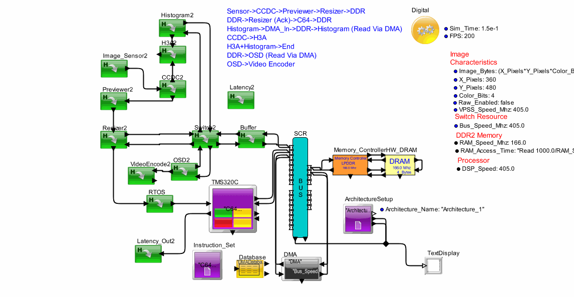
The Video Processing Front End creates new images based on top level parameters in the model:

(1) X_Pixels
(2) Y_Pixels
(3) Color_Bits
(4) Raw_Enabled

The last parameter sets a field of the image data structure, called A_Raw_Image to true or false. The first three determine the image size in Bytes by the Image_Bytes parameter:

(X_Pixels*Y_Pixels*Color_Bits)/8

This precalulates the image size, which is then placed in the Image_Sensor data structure. The image arrives at the CCDC hierarchical block. Inside the CCDC hierarchical block it sends a message via the 32 bit configuration bus that an image has arrived. The 32 bit configuration bus then sends the message to the RTOS block, which in turn executes a control CCDC task on the ARM processor. The control task is generated in the Instruction_Mix_Table from the SoftGen. When this control task completes on the ARM, it returns to the RTOS block, which then sends register updates to the CCDC block, and processes the incoming image.

There is a delay for the register updates, then the image is processed in the CCDC block, based on the Image_Bytes value:

Cycle_Time*(Image_Bytes/Width_Bytes)

where cycle time is clock period of the CCDC block. This block also keeps track of how many times the H3A image has been sampled by a value set in the InitMemory block. If the field Sample_Count is incremented and if the Sample_Max (InitMemory value) is reached, then Sample_Count is set to zero. The CCDC blocks sends the image to the buffer, H3A and iPipe blocks.

Inside the Buffer, connected to the 64 bit bus, the request is fragmented into 64 byte write bursts and sent to the SDRAM_1. Inside the H3A and iPipe blocks, there is processing of the CCDC image, based on the conditions. The image arriving at the H3A sends a message to the RTOS, like the CCDC, indicating an image has arrived ready to be processed. Similarly, the image arrives at the iPipe and sends a message to the RTOS via the configuration bus.

If the H3A Sample_Count field of the arriving data structure is 0, signifying that this image should be processed, it will set the processing delay to a positive value, else it will set it to zero. Like CCDC block, the H3A block waits for the ARM processor to send a message to start processing. Once this message is received, it models the register update time, and the processing time. The processing time can be 0.0 for a non-sampled image. In addition, if the processing time in the field DELTA is 0.0, nothing will be sent to the buffer.

The iPipe will also wait for the ARM control task to complete before it performs it's processing. Currently, there is no logic for the type of processing the iPipe will perform. It could perform a raw to YCbCr conversion, subtract a dark frame, or send to SDRAM_1, for example. For now, we just use a simple delay.

Once, all of the 1/30 sec image has been processed one can calculate the time margin (positive value) or time deficit (negative value) of the original image:
Delta = TNow - input.TIME
Frame_Delay = "Frame_Delay = " + (Frame_Time - Delta)
where Frame_Time will be 1 / 30 of a second, input.TIME is the original image time, TNow is the current simulation time.

The ARM processor is a 926. The cache size and clock speed can be modified. The processor gets the instruction and data from the SDRAm, connected to the 64-bit Bus.

The DMA is added to the 32-bit and the 64-bit Buses. This model is currently not using the DMA.

The 32-bit bus is used to communicate between the CCDC, H3A and the iPIPE with the ARM. The 64-bit bus is used to communicate between the Buffer logic and the SDRAm; and the ARM and the SDRAM.

Click here to view the pdf